-
 teleko7
0Hi all
teleko7
0Hi all
First of all, thanks and congratulations to all the people in MW101. I think this is in the top 3 (#1) of the MW resources out there!!
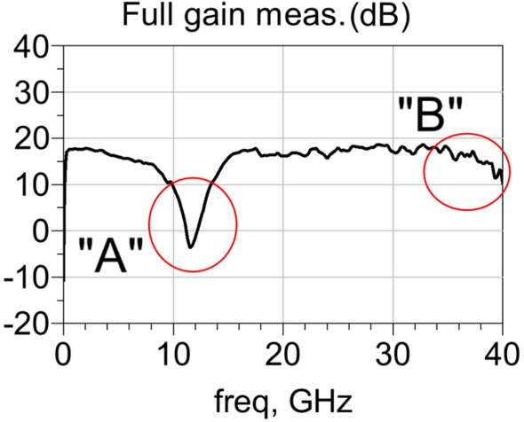
I've designed and fabricated my forst version of a 1 to 40GHz DA MMIC (GaN on Si), with 20dB gain and Pout >1W P1dB for the whole bandwidth (hopefuly). Input and output match is good, gain is decent (some 17-18dB, with Vgs-s still to be tuned due to differences in Vth and Idss from EM simulation to measurements) and I still have to measure Pout.
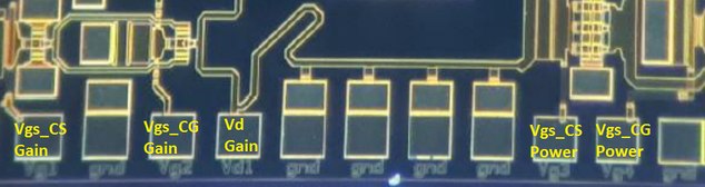
BUT, There's a naughty absorption in my S21 measurement around 12GHz (the "A" dip in the first picture). My amplifier consists of 2 series connected cascode DA stages, one for gain and the second for power. I've checked in EM simulation that this effect is due to my first stage being loaded by the DC bias external circuitry (drain bias is applied to both sides of the drain line of stage #1, second picture).
When I apply bias to the second stage I also see this loading, if I apply it through the drain termination side. Only applying bias voltage directly through the output pads with a bias tee can I avoid this effect... And only in the power stage... And here comes the question...
Thinking about it, I would expect this effect to be present in every wideband distributed amplifier, as bias bondwires and the capacitance of the PCB areas where they land will resonate in the GHz range (be it higher or lower). But I have seen several papers of amplifiers with equal or higher bandwidths (though with lower power and gain) for similar and even higher frequencies that don't have such absorptions in their S21 response. What is more, some apply bias with only a line section with a capacitor (lambda/4 for several decades???), and this puzzles me completely, as I would expect those designs to behave like mine... What am I missing? Is it a matter of output line impedance (I guess most of us work with 50 ohm)? Do they use 4mm long bondwires or what? Because I guess they will have to encapsulate and somehow bias their MMICs for their final applications also...
And regarding my biasing problem... Any suggestions? I'm reading about using transistors as active sources but to be honest I've used some 85% of my MMIC area and don't think I'm going to be able to include anything substantially "big" in my design, so I need to think "out of the MMIC"... I'm trying to take resonances down below 1GHz but it doesn't seem to be easy...
Anyway, sorry for my dissertation and thanks again to all of you for reading this :smile:
IbanAttachments S21
(89K)
S21
(89K)
 Stage1DrainBiasRight
(721K)
Stage1DrainBiasRight
(721K)
-
 UnknownEditor
5I have never designed a distributed amplifier so I don't have any great suggestions except look at spiral inductors for the drain supply line.... also, if you send me an email I can send you a presentation that you might find valuable
UnknownEditor
5I have never designed a distributed amplifier so I don't have any great suggestions except look at spiral inductors for the drain supply line.... also, if you send me an email I can send you a presentation that you might find valuable
Steve
unknowneditoratmicrowaves101dotcom -
 Nguyen
0Hi Iban,
Nguyen
0Hi Iban,
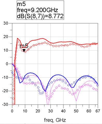
I just ran over your post today and I want to share my results as well. In fact, you were right on the dip at around 10-ish GHz. I have seen many papers reported this effect. I have designed several DAs and use very simple single wire bias choke since I didn't care about what's going on below 20GHz. You can see that I also have that dip at 10GHz.
There's a paper out there claiming that they use a structure of high Z line - spiral inductor - high Z line, that can create a very good RF choke. But I can't pull out which paper it was at the moment. I will try and keep you posted. Otherwise, if your chip consumes not >150mA, there's off-chip RF choke out there that can handle upto 50GHz for a pricey cost.
It would be great if you can share a way if you figure it out. I am also interested in this.
Thanks,
NguyenAttachmentsBias
(639K)
 Meas
(10K)
Meas
(10K)
-
teleko7
0Hi Nguyen
Sorry for my late reply, I've been doing some work on this issue and I forgot about MW101 for a while...
The problem is the resonance between the wirebond's L and the parasitic C of the PCB area where it lands. This resonance lies in the 7-15GHz range, as you know.
I've tried to take it out of my BW (1-40GHz) by using very short wirebonds and thin, high permittivity substrates with wide PCB areas and SMD capacitors (fres>40GHz), but no way.
In fact I have kind of a "solution" (which I don't like much but it is my best bet up to now...): I'm using a single 4mm - 5mm long wirebond (1mil diameter, gold) on either side of my DA's gain stage drain line.
What I've managed to do is to make the resonance go below 1GHz by using theses long wirebonds and Dicap Capacitors (100pF, 12mil wide).
With 4mm, the gain is still affected by some 2dBs at 1GHz (6mm would be nice but impractical). My main concern with this solution is the maximum current my wirebond can withstand... I need about 350mA for the gain stage drain line. I've been reading some papers and documents on the subject and I think that 300mA (200mA more realistic) is the highest current I can achieve for this wirebond legth and diameter... And more wirebonds reduce inductance, increasing fres... Anybody, any help or comments on this?
I've analyzed Coilcraft's conical inductors also, but the PCB pattern they require for soldering makes the resonance show up in my simulations (even halving the area of the smallest one)...
At present I'm also considering Vishay's RFLW 3 and 5 series of wirebondable spiral inductors. Thier SRF falls below 6GHz but if I manage to concatenate a couple of them with shorter wirebonds this could make my day... I'll try to get samples or buy a few (but there seems to be no stock for my country, Spain). The problem with this is delivery time, as I need to carry out measurements right now...
This DC supply issue in wideband amplifiers is a topic I haven't seen covered much in papers out there. We'll publish a simple paper at our URSI meeting this september, but only scratching the surface of the topic... I'd thank if somebody could forward me titles of publications concerning this issue.
All help is welcome. I'll post my advances and measurement results ASAP.
Thanks for reading.
Iban


Welcome!
Join the international conversation on a broad range of microwave and RF topics. Learn about the latest developments in our industry, post questions for your peers to answer, and weigh in with some answers if you can!
Categories
- About Our Site
- Antennas
- Applications
- Biological Effects and Applications
- Calculators
- Communications
- Computer Aided Design
- EDA Software
- Emerging Applications and Technology
- Employment
- Field Theory
- Filters and Passives
- General Questions
- High Power
- History
- MMIC and RFIC
- Packaging and Materials
- Radar
- Sources and Receivers
- Test and Measurement
More Discussions
- Terms of Service
- Useful Hints and Tips
- Sign In
- © 2026 Microwaves 101 Discussion Board