Comments
-
wire and coax impedanceI didn't know about the heavy frequency dependence, thanks for that! I agree that ImAg is definitely the best passivation for loss, but HASL is a close second (if you can put up with the non-planarity of the pads).
I totally agree that ENIG is not harmless. If the ur is ~1 at higher frequencies, I wonder if it comes down to the bulk conductivity of Ni not being great.
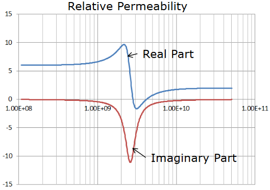
I once found this (single point experimental) data on the permeability of eNi which, looking back on it, supports your assertion of negligible permeability >10GHz
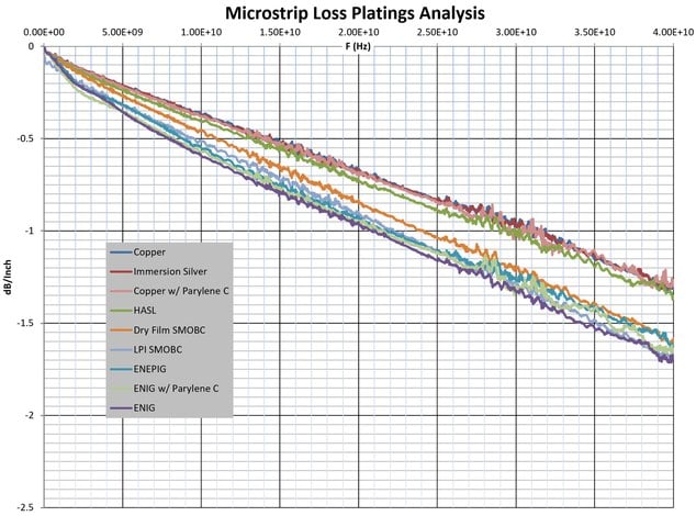
I've also attached an experiment I did with multiple platings on the same board geometry as a passivation loss comparison out to 40GHz. It's obvious that anything with nickel in it is worse. Also note how the loss slope of nickel platings is really steep until ~2GHz and then straightens out. Another piece of evidence of the 2GHz inflection of nickel's permeability!Attachments Electroless Nickel Permeability
(31K)
Electroless Nickel Permeability
(31K)
 Microstrip Loss by Plating
(448K)
Microstrip Loss by Plating
(448K)
-
wire and coax impedanceNow seems like a good time to point out that Electroless Nickel (such as in ENIG finishes) is not pure Ni but instead contains "high phosphorus content" typically around 10% P, this effectively makes the Electroless Nickel alloy non-magnetic with a relative permeability mu_r near 1. This is a common electrical simulation mistake where designers might assume electroless nickel has the same properties as pure nickel with a mu_r in the many hundreds.
Another side note, the bulk conductivity is also much worse than pure nickel...
I personally use mu_r of 3, and a resistivity of 60 uOhm-cm. -
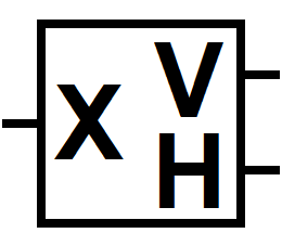
OMTsSymbols are usually derived from either the mathematical symbolism of the operation they perform or from the physical shape of the common implementation of mechanism.
For an OMT, there isn't really a graphical description of the mathematical operation and the physical shape of an OMT is really just a bunch of rectangles...
I think in this case it makes sense to fall back to a Box with a reference to port functions, i.e. A square bounding box with an O, X, or large + to represent the dual-pol port. The O would be for circular waveguide (but sometimes people will use a square waveguide), or perhaps use an X for cross-polarized or use a large plus for a physical representation of horizontal and vertical polarization superimposed together)
The polarized ports can simply be described by a V or an H to clearly indicate the two single-pol ports. (Or L and R if you're doing circular polarization...)AttachmentOMT Symbol
(2K)
-
DC biasing connection on MW LNAsThe DC pins are typically hermetic feedthrough pins (although not always hermetic). They frequently also incorporate a Discoidal Capacitor for decoupling. Sometimes they're soldered in, sometimes they're laser welded in, sometimes they're screwed into a tapped hole, but they're always intended to be soldered to a wire (usually covered with heatshrink when you're done, gotta keep it tidy!)
As for the ground lug, they're always screwed in because who would want to go through the trouble of laser welding something that has no internal pin connection? I have no idea why they have the little flare at the end of the pin though... maybe it's just to make it extra easy to grab with an alligator clip?


CMoncsko

Start FollowingSend a Message
- Terms of Service
- Useful Hints and Tips
- Sign In
- © 2026 Microwaves 101 Discussion Board